
Medical Digital Radiography Solutions
What is Digital Radiography?
Digital Radiography is the next technological advancement to replace CR systems in the Radiography industry. Digital Radiography technology uses a combination of X-Ray and light sensitive plates that are then picked up by a detector panel and stored as an electric charge. The charge is then converted into decimals and turned into a readable image.
Because X-Rays taken with Digital Radiography panels can be instantly converted into an image, DR technology can greatly streamline work processes as there is no longer any need for a cassette medium that needs to be read and converted in a CR System. Which can be time consuming at best even with high-end CR machines.
Different types of DR Panels
As is with most other technologies, there may be more than one method to achieve a similar result, this can also be said for Direct Radiography as well. The 2 main types of digital radiography are comprised of, Direct and Indirect conversion methods.
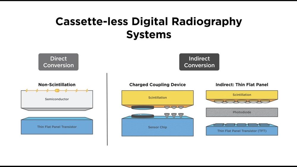
Indirect Conversion
Thin Flat Panel Transistor (TFT)
TFT Panels are comprised of three main layers. the Scintillation layer, the Photodiode layer and the TFT array.
Scintillation Layer: The Scintillation layer also known as the light later sits at the top of the 3 layers. When a photon from an X-Ray for example hits the Scintillation layer, it creates a small burst of isotropic light. The down side is that this burst of light in all directions can cause a decrease in spatial resolution as the light particle would be of a greater size than the photon.
To combat this, Scintillation layers are commonly made out of either Cesium Iodide (CsI) or Gadolinium oxysulfide (Gd). Cesium Iodide being the preferred material in the industry, is produced into small rods that focus the light more efficiently, thus increasing the brightness and resolution of your image. Gadolinium although cost effective and easier to produce, isn’t as good at focusing light than Cesium Iodide.
Photodiode Layer: The Photodiode Layer is made up of amorphous silicon, a Semiconducting material capable of converting incoming light photons from the Scintillation into an electric charge. These electrons are then passed on to the TFT Array.
Thin Film Transistor layer (TFT): The TFT layer consists of an array of multiple, very small detectors also referred to as DEL’s. Each DEL then contains a Pixel detector, a storage capacitor and a switch. The electrons from the Photodiode layer are captured by the pixel element and moved to the storage capacitor. The switch then opens or closes the release of the electric charge produced by the DEL allowing the computer to read the information produced by the panel.
Charged Coupled Device (CCD)
A charge-coupled device can either be an area array (square) or linear array (rectangular or 'one-dimensional'). It comprises discrete detector elements (dexels) that have a photosensitive area made of amorphous silicon and an electronic component. The space taken up by these electronics results in decreased absorption efficiency as this portion of the dexel will not be photosensitive. CCD chips are small, for example, 40-60 mm2, when compared with a standard radiographic field of view, and the demagnification of the image contributes to the inefficiency of the system.
Direct Conversion
Non-Scintillation Panel
Non-Scintillation detectors use a thinly layered amorphous selenium, which is an X-Ray photoconductor converting X-Ray protons directly into an electric charge. This charge is then received by the TFT (Thin Film transistor) array which captures the electric charge and converts it into a digital signal and sends it to a storage capacitor to be sent and read by the computer software.
Main Factors to consider when buying a Digital Radiography Panel
When investing in a product as important as a DR Panel it is paramount to be across all the variables regarding this new technology. Below is a list covering the more important specifications and their definitions.
Detection Method
As briefly explained above, your detection method describes how your DR Panel operates. Both methods have their pro’s and con’s however as of the market today it is shown that indirect conversion methods provide a sharper image compared to direct conversion.
Pixel Size (µm)
Pixel Size represented by microns (µm) describes the distance between each pixel. The lower the number the better as this represents a sharper quality of image.
Image Area Size
Image Area Size is how much of the panels area is used for the image. This is a good measurement for showing how the panel makes use of the space available. Compare this measurement with the panel’s external dimensions.
Cycle Time
Cycle time indicates how fast the Panel is at transferring the image from the panel to the computer. The lower the time the faster the work process for employees.
Now that you understand some of the underpinning ideas to Digital Radiography Panels click the button below to view our high-quality selection of DR Panels that we have on offer.
